Revolutionizing Electronics: The Quest for Lab-Grown Diamonds
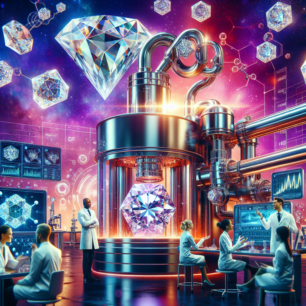
**Lab-grown diamonds** are becoming a critical component for advancing future technologies in electronics, optics, and sensors. Researchers at the DOE's Princeton Plasma Physics Laboratory (PPPL) and Princeton University are innovating ways to grow high-quality diamonds at lower temperatures, making them suitable for use in silicon-based manufacturing. **Diamonds offer unique properties** like heat dissipation and the ability to withstand high electrical voltages, making them valuable for the semiconductor industry. The study addresses the challenges of traditional high-temperature diamond growth, which can be damaging to computer chips. By focusing on plasma-enhanced chemical vapor deposition, the researchers identified a critical temperature above which acetylene aids diamond growth while avoiding soot formation. This discovery is paramount in refining diamond growth processes. Additionally, the study delves into hydrogenation of diamond surfaces, crucial for creating diamonds with nitrogen-vacancy (NV) centers. These centers are beneficial for quantum applications due to their ability to hold more information than regular bits, making them excellent for sensors. Research explored alternative hydrogenation techniques like forming gas annealing and cold plasma termination, which could improve results while preserving NV centers. This cutting-edge research takes place at the newly established **Quantum Diamond Laboratory** at PPPL, indicating further explorations in diamond surface preparation for quantum computing and sensing. The study emphasizes a blend of traditional and innovative methods, aiming to write a 'recipe book' for producing optimal hydrogenated diamond surfaces.